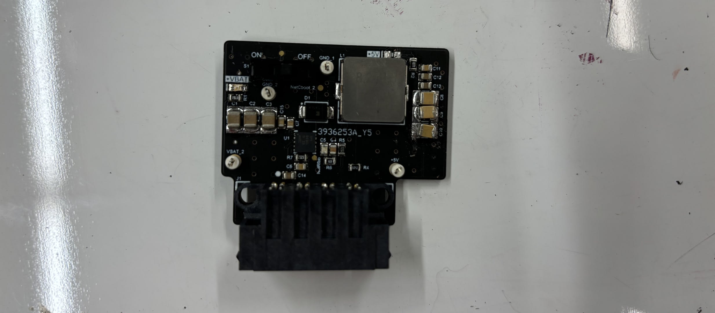
Power Distribution Board (PDB)
Background
This project was completed for the University of Waterloo Robotics Team’s 2023/24 Mars rover.
The PDB is the most critical custom PCB on the rover. It is responsible for accepting 48V from the battery and distributing 48V to the drive train, converting (48-17V) and supplying power to out main computer a Jetson Xavier and converting (48-5V) and supplying power to our science module. Without a functioning PDB, our electrical architecture becomes very messy and bloated trying to use off the shelf parts to replace this single compact board.

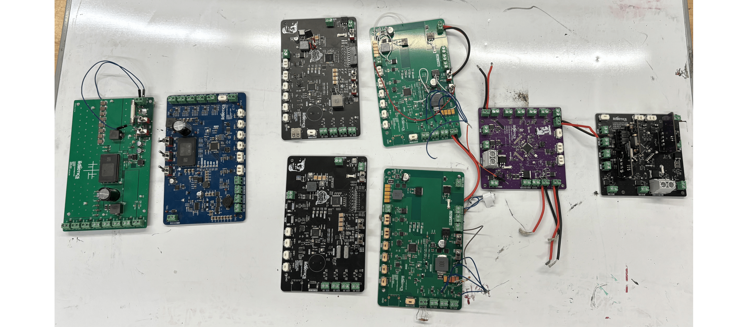
Unfortunately, this is exactly what we had been doing for years. This revision of the PDB is technically the 5th full redesign of the PDB and not a single one of the previous 4 revisions worked well enough to be used in the rover.

Having been the electrical lead for a year and overseen two of these failed revisions, I felt personally responsible for the failure to provide the team with a working board. I made it my mission to get a working PSB by the end of summer 2023.
The Plan
Before starting this new revision, I took some time to think about why all the previous revisions had failed. I was able to narrow it down to the following factors:
- The board was too large and complex for a revision to be completed by a single person in a single semester.
- The size of the board made it cumbersome to properly review in design reviews.
- The assembly and testing of the board took forever and were usually completed by someone other than the designer.
- The on board buck converters were a consistent point of failure that made the whole board unusable.

Architecture Changes
My plan was to reduce the complexity of the board by removing as many of the unwanted submodules as I could. I had a meeting with the other team leads where we boiled the board down to it’s core features:
- 5V Power Conversion/Distribution and Load Monitoring
- 17V Power Conversion/Distirbuition and Load Monitoring
- 48V Power Distribution and Load Monitoring
- LED Control
- CAN
This meant removing the on-board temperature sensor, the USB port and the ultrasonic sensor support. None of these features were critical to the rover’s overall functionality so we got rid of them.
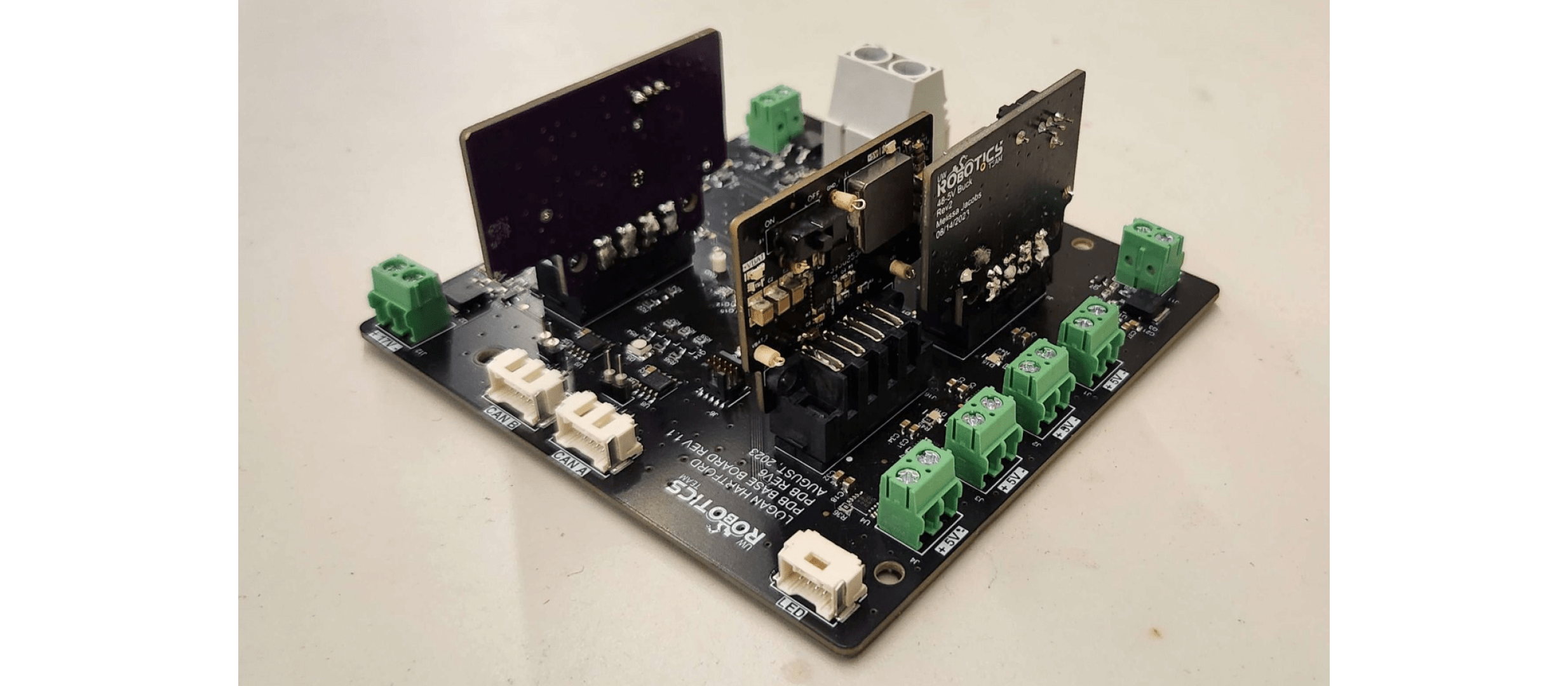
Even without these features, the board was still massive and quite complex and would be difficult for my to complete by myself. I realized I needed a way to bring more people in on the project. This is what inspired the modular design you see above.

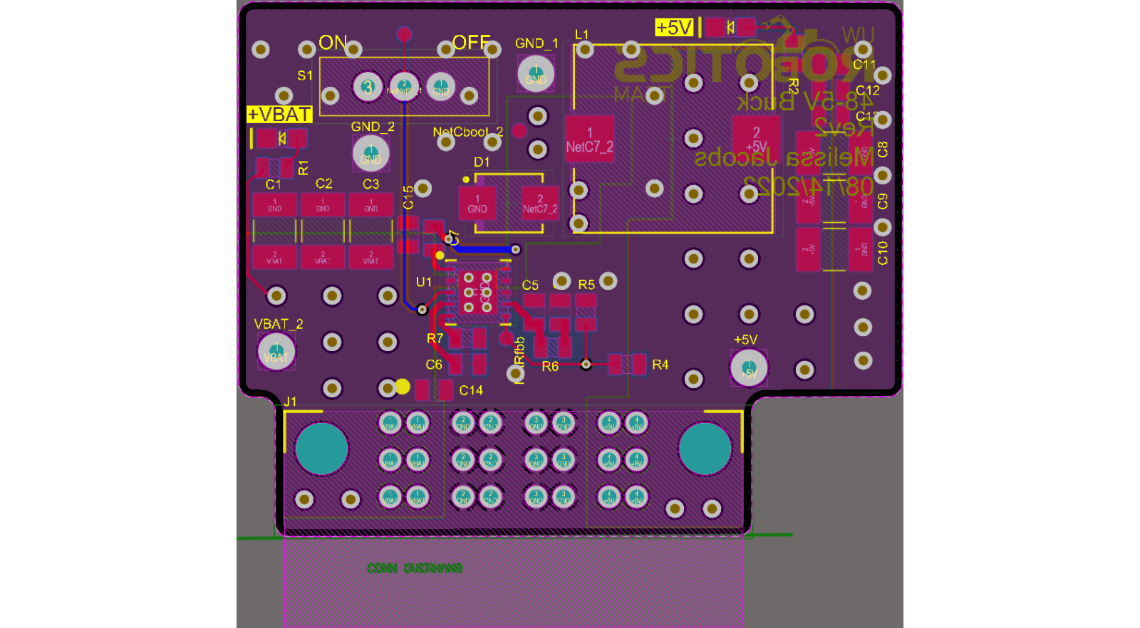
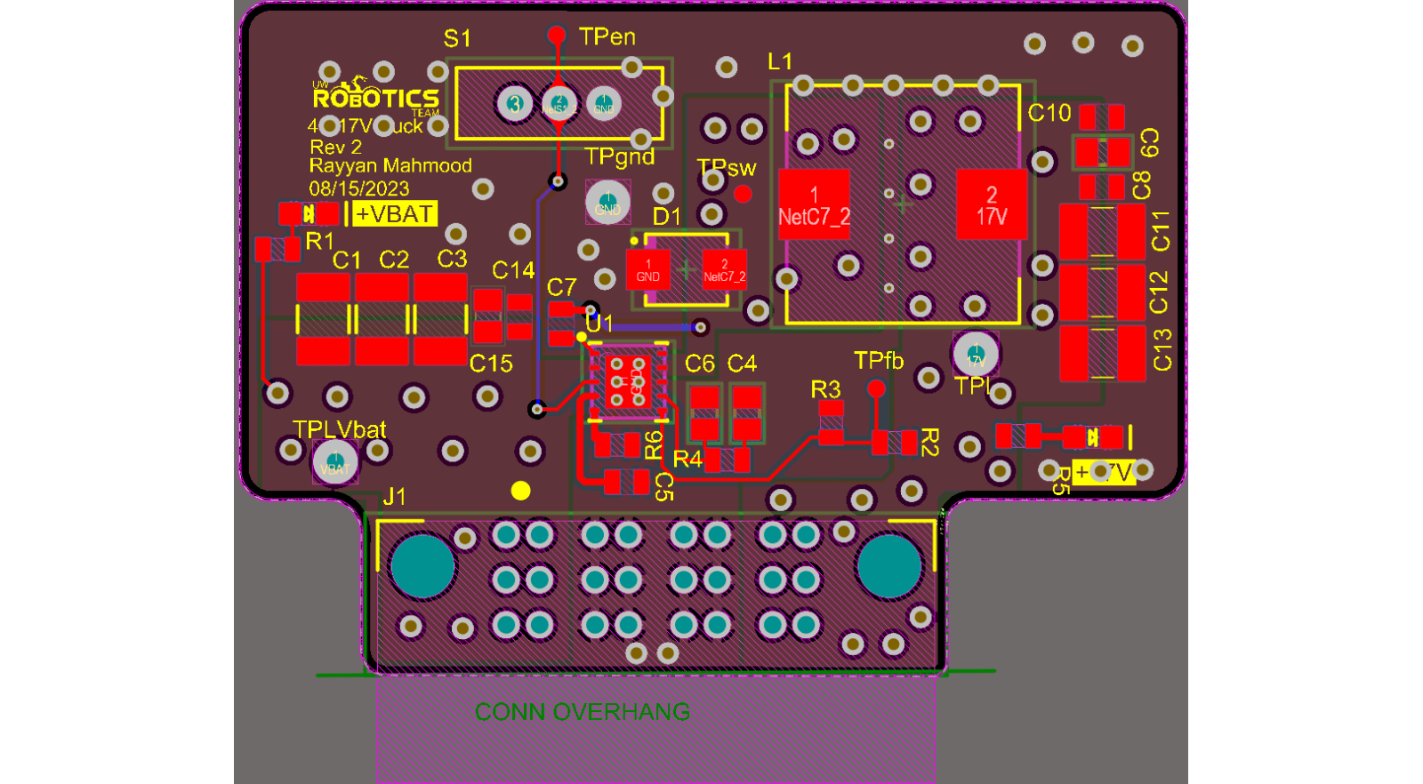
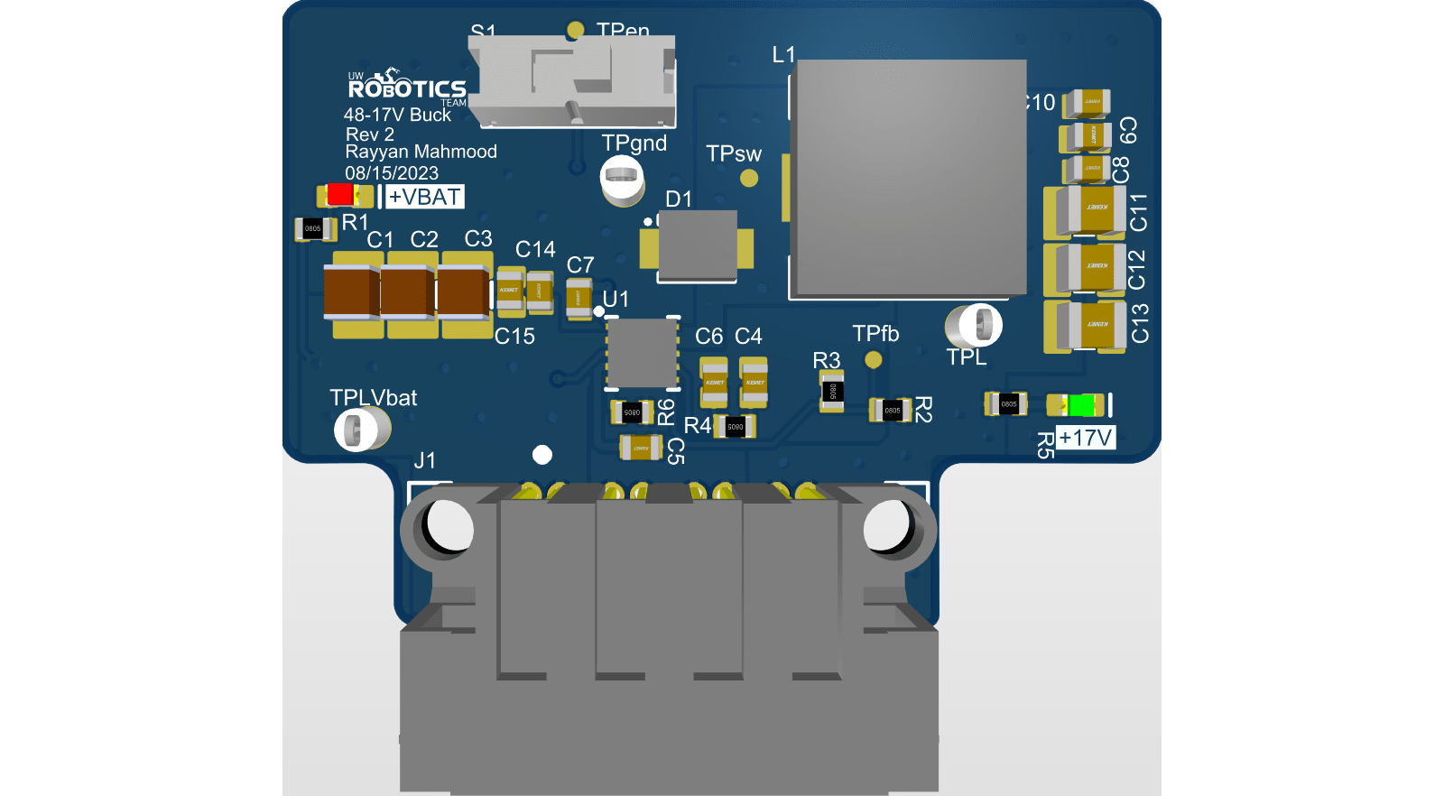
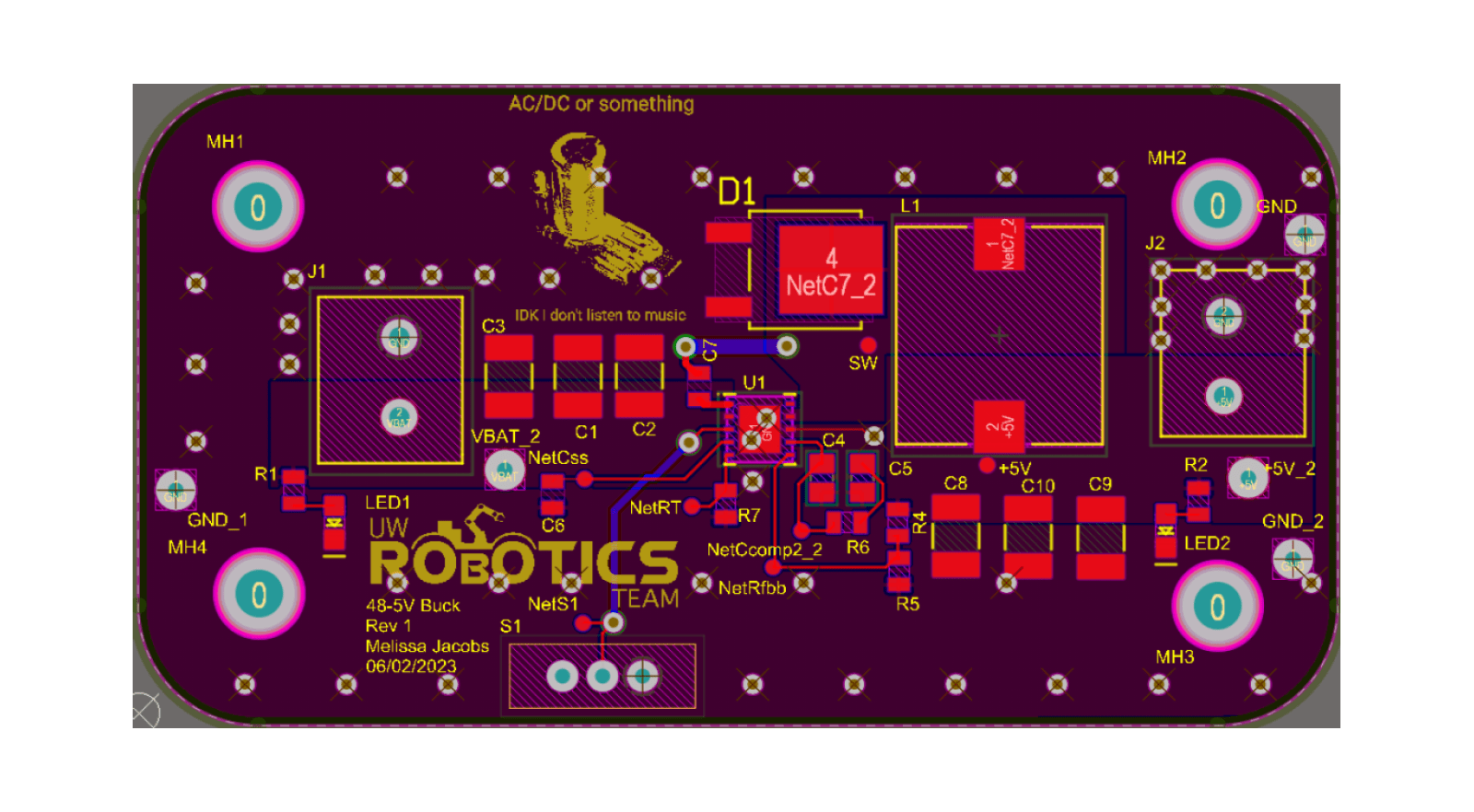
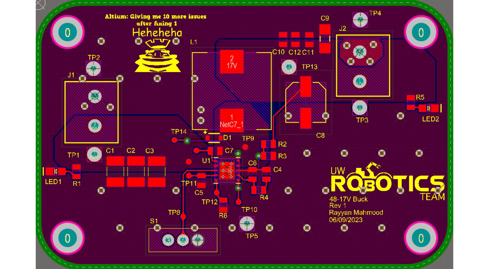
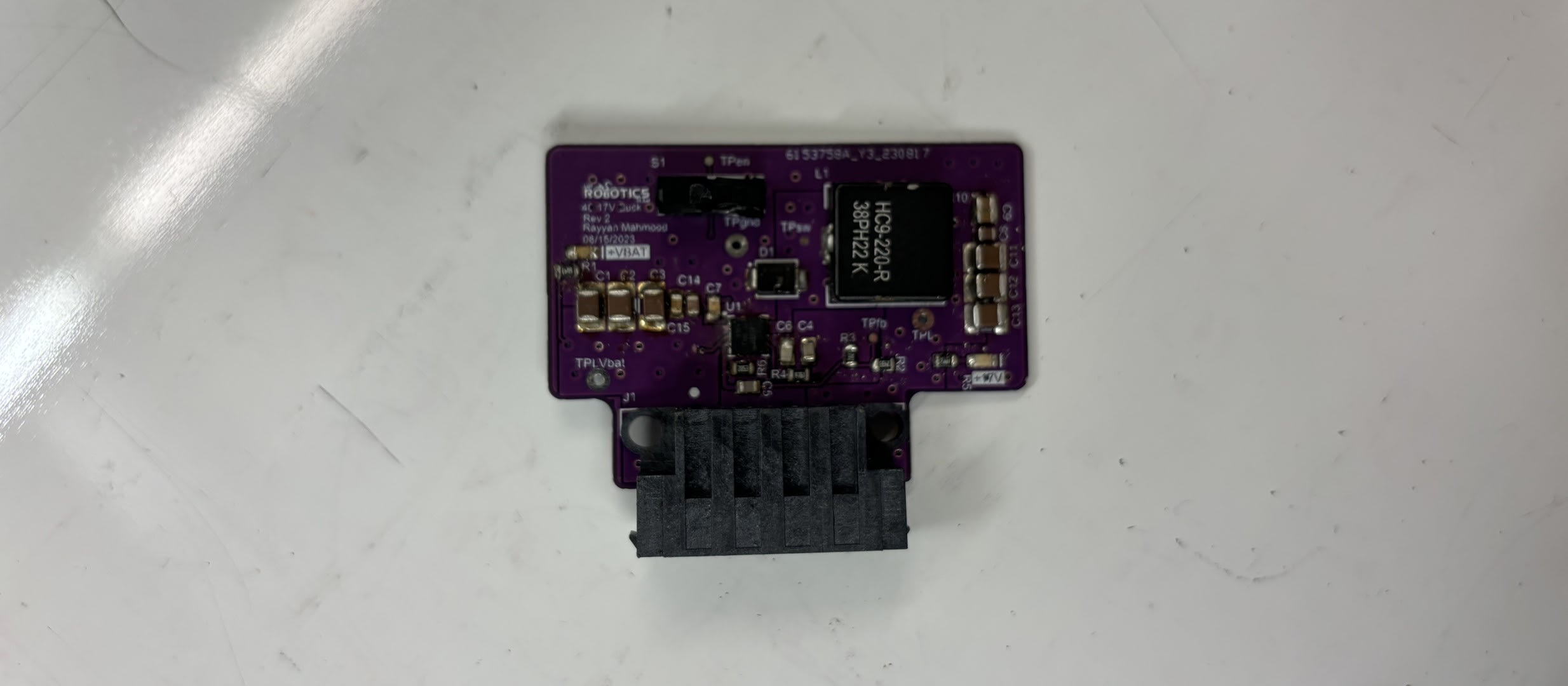
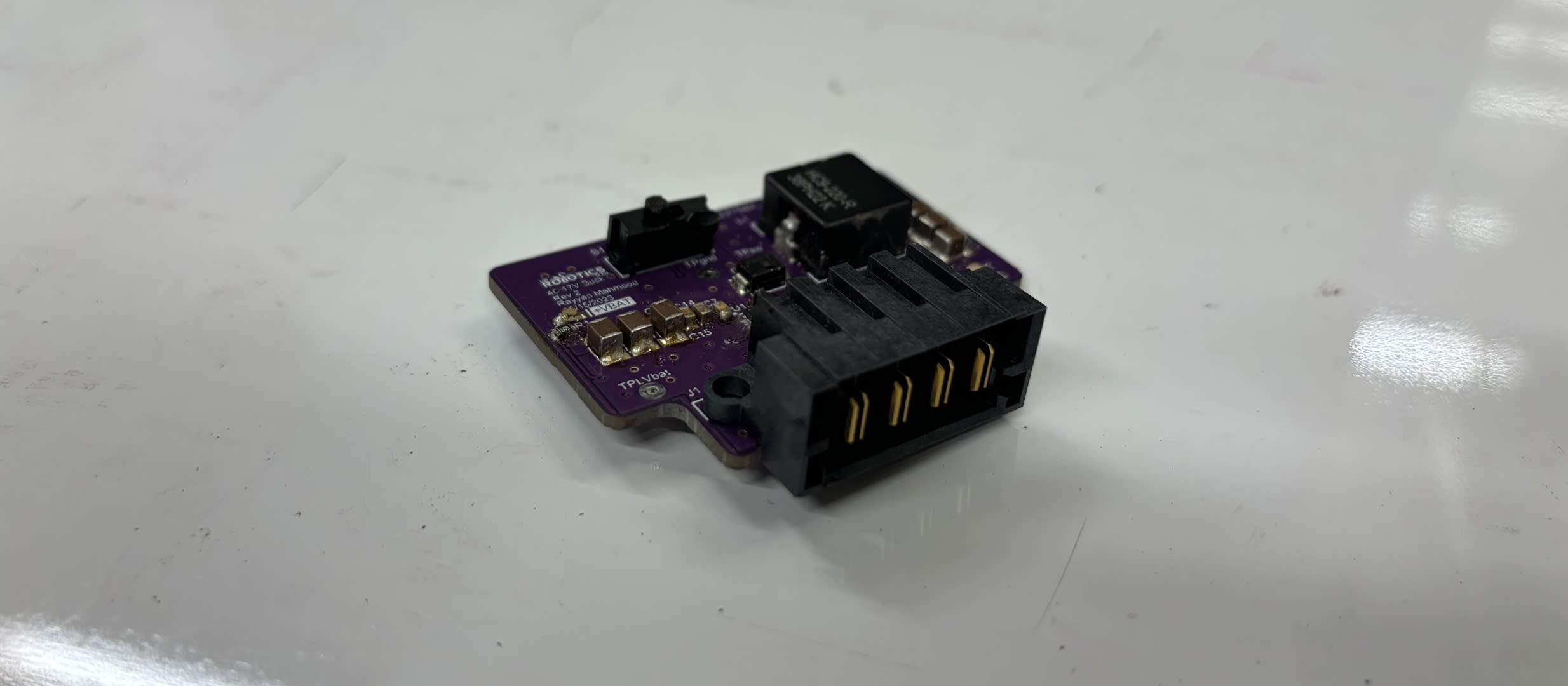
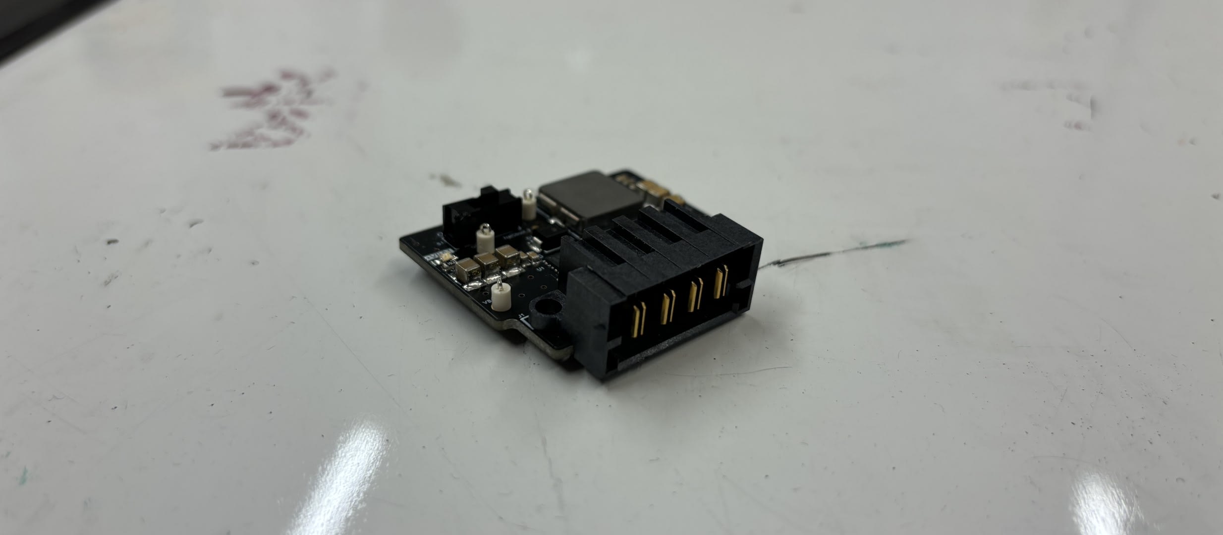
I decided that we should break the board up into 3 parts that could be worked on by 3 people in parallel. I decided to breakout the buck converters since these modules tended to be the hardest to develop and were most likely to fail. With this architecture, an issue on the 5V buck would not render the whole board useless, we could simply swap modules and continue. The buck converters would connect to the baseboard vie Board-to-Board (B2B) connectors which would supply the modules with 48V and return the bucked voltage from the modules.
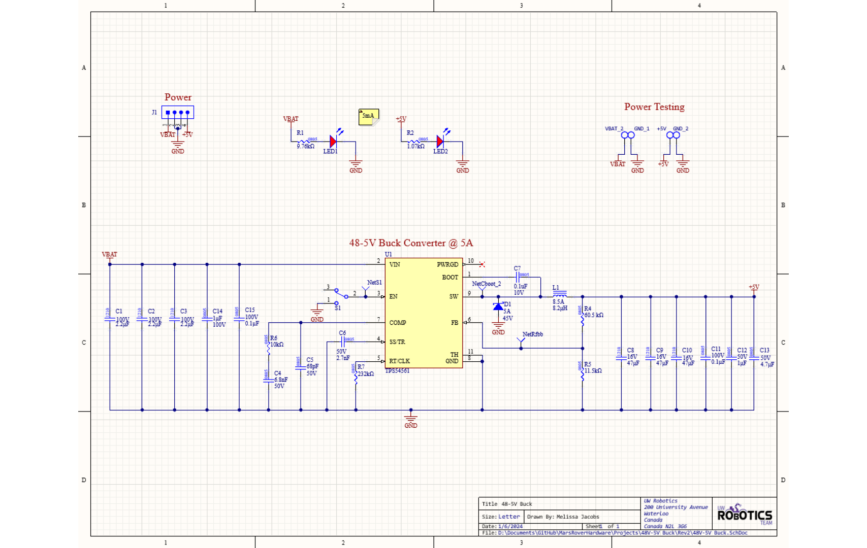
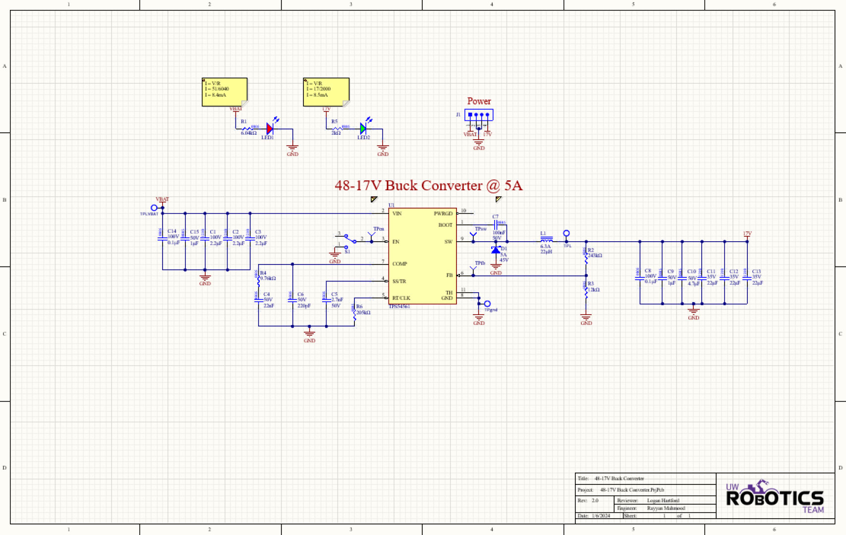
We decided to do the 5V power conversion using 2 bucks in parallel since we would require 10A@5V and designing two 5A controllers would be easier than designing a single 10A buck. We did not have to worry about any interference from the two bucks since we could separate the 5V distribution into two separate channels. The 17V buck only needed to be able to supply up to 4A so we did this in a single converter.

I had a vision of making the buck modules clip into the baseboard vertically like RAM into a motherboard. I wasn’t exactly sure how I was going to do it yet, but this seem like the most space efficient way to create this modular system.
Grind Time
Even with the workload divided, I new from past experience that it would likely take two revisions of each board to get them perfect which is difficult to do in one semester. I asked the electrical team who would be interested in working with me on a project that would require a lot of their time and attention and Rayyan Mahmood and Melissa Jacobs eagerly volunteered.

We decided to name the project PDB Grind as we were going to start working on the project even before the semester started and put in some full days designing the boards together. We also committed to working as much as we could in our spare time and working collaboratively for a full day each week.
Melissa was going to work on the 5V buck converter, Rayyan would work on the 17V buck converter and I would work on the baseboard which the buck converter modules would plug into. Since this was Melissa and Rayyan’s first PCB designs, I created these Board Development Paths for them to follow as they completed their designs and for me to track their progress.
Baseboard Schematic
The baseboard schematic is broken up into 6 sheets:

- 48V Power
- 5V Power
- 17V Power
- 3V3 Power
- Microcontroller
- CAN
My first order of business was removing all the unnecessary components from the schematic and generally cleaning them up. Next I focused on implementing the core design features, making changes to the design only where necessary
48V Power
The previous revisions did not have any load monitoring for the 48V system. To protect our 48V motor drivers (ODrives) which are very expensive, I added a terminal for each of the 3 ODrives on the rover and gave them each a load monitoring circuit.

The load monitoring circuit is composed of a current sense IC and a highside load switch. The current sense IC has two current sense inputs which connect to the terminals of a current sense resistor which sets the current limit. If the current being supplied to the ODrive exceeds the current limit, OUT will go from low to high. The STM32 monitors this pin and shuts of the output by disabling the load switch.
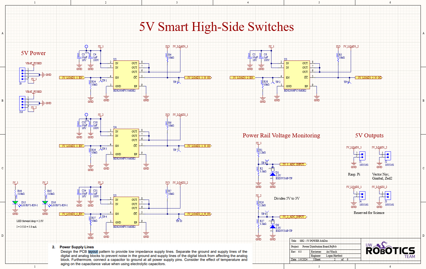
5V Power
In the previous revision, the 5V system had been broken into 4 outputs, each monitored by a smart-highside switch. These switches worked in in the last revision so I left them as is. The main change to the 5V system was the removal of the buck circuit and the addition of the B2B connector.

The connector I went with was a Samtec PowerStrip. I chose this connector due to its high current rating (30A per pin) and because is large size and mating surface area would provide more stability to the vertically mounted buck converter modules. The vertical connector on the left would live on the baseboard and the right angle connector on the right would live on the buck modules.
Note: In the first revision of the baseboard, I did not include this connector. Since the baseboard and bucks would be tested and developed in parallel, I added terminals to supply 5V from a power supply to the baseboard to allow for easier testing.
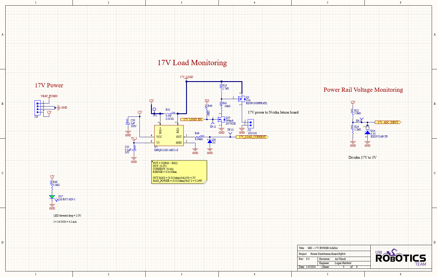
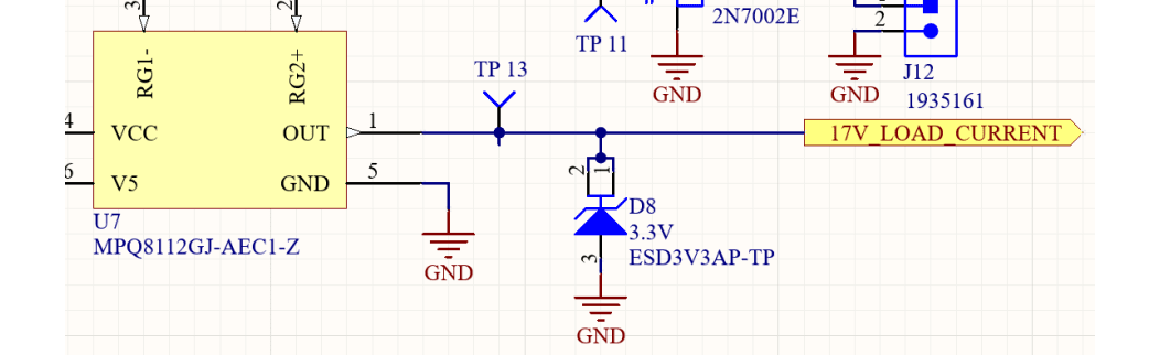
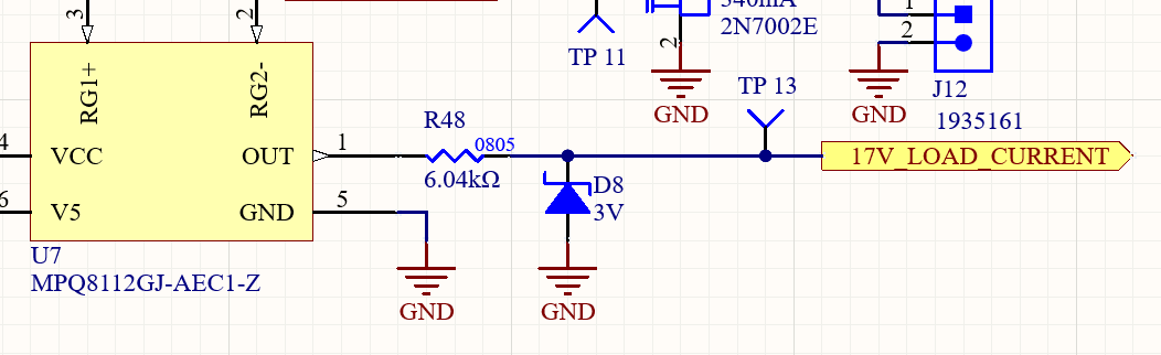
17V Power
The 17V system had load monitoring in the previous revision but it did not work. I changed the load monitoring to the same current sense IC and high-side load switch configuration as for the 48V system. I only needed to adjust the current sense resistors and load switch MOSFETs. I also removed the 17V buck circuit and added in the B2B connector.
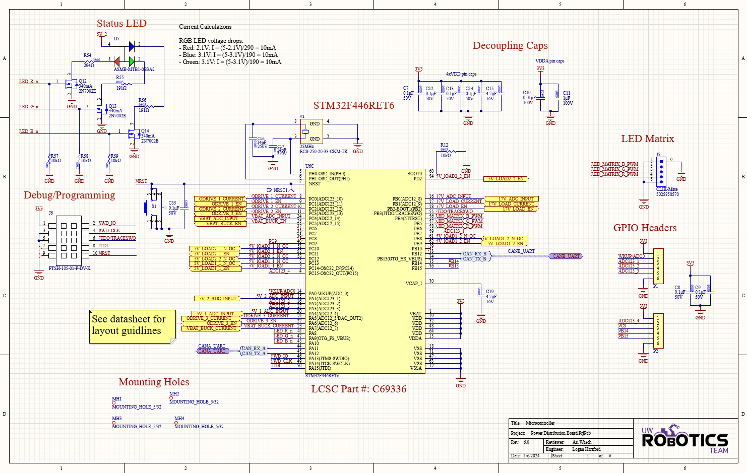
Microcontroller
I changed out the RGB status LED since the one on the previous revision did not work. I also removed the temperature sensor circuit and the USB connector.

The main addition to this sheet was a set of GPIO headers to breakout the unused pins on the micro. This would allow old or partially broken baseboards to be used a mini STM32 dev boards.
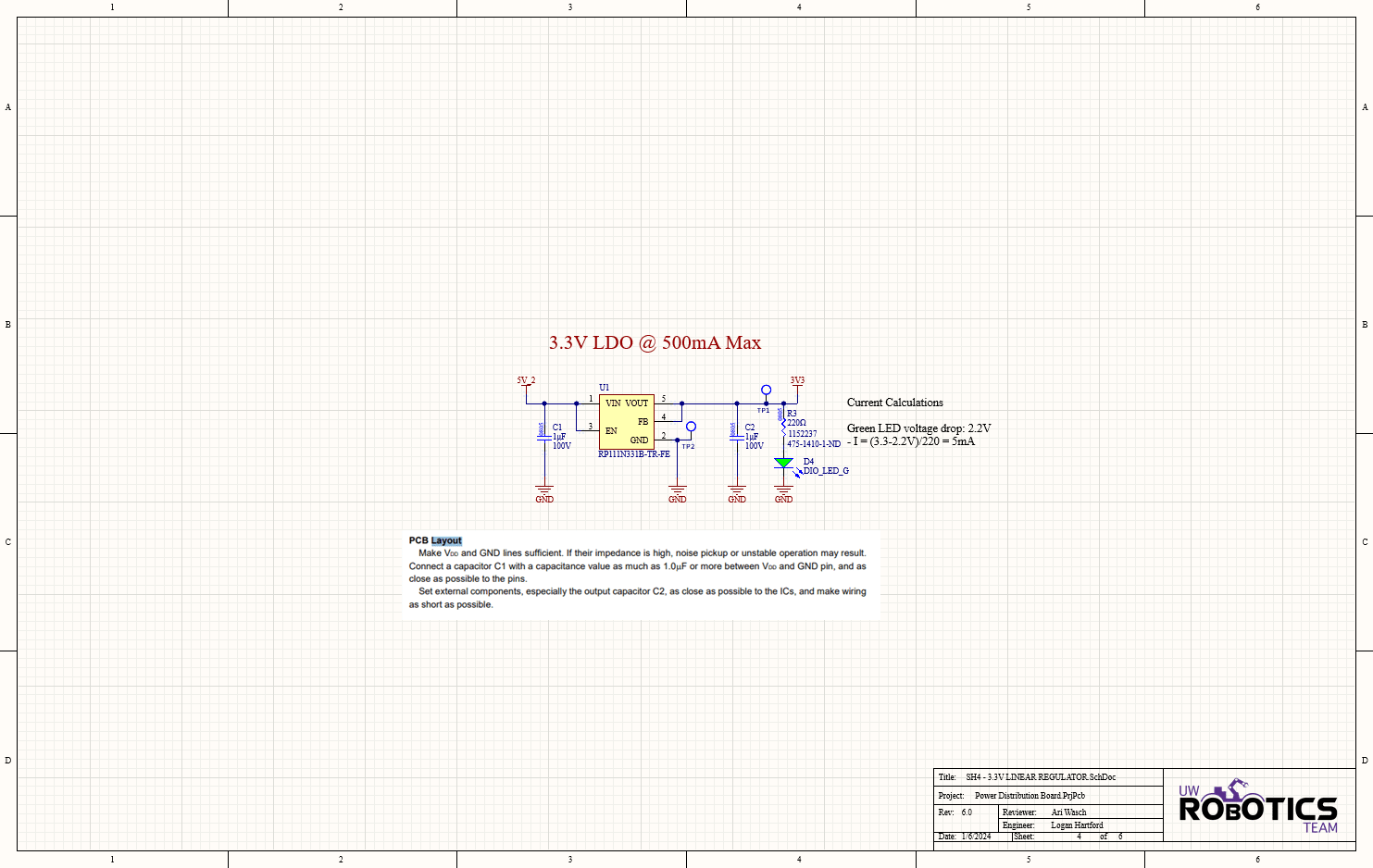
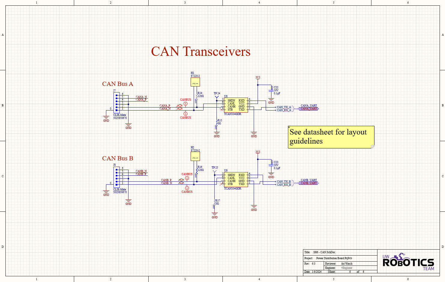
CAN and 3V3
The CAN transceiver and the 3V3 circuits were common to many of our designs and known to work so no work was needed on these schematics
Buck Module Schematics
The schematics for the 5V and 17V buck converters were created by Melissa and Rayyan respectively. They generated their designs using WeBench (5V | 17V) and then transferred to Altium.
My contribution included teaching them how to use WeBench and how to select a good design. I told them to choose designs that would be simple to implement, low cost and had at least two layout references. Additionally, I was teaching them how to use Alitum including how to create new library parts and how to make a readable schematic. I encouraged them to do their own calculations and verify the WeBench design and I was the main reviewer of their schematics.
Baseboard Layout
I did the layout for this revision from scratch as the layout from previous revision was messy and contained useless artifacts from previous design. The layout for this design is simple, there are just a lot of components and connections to make.
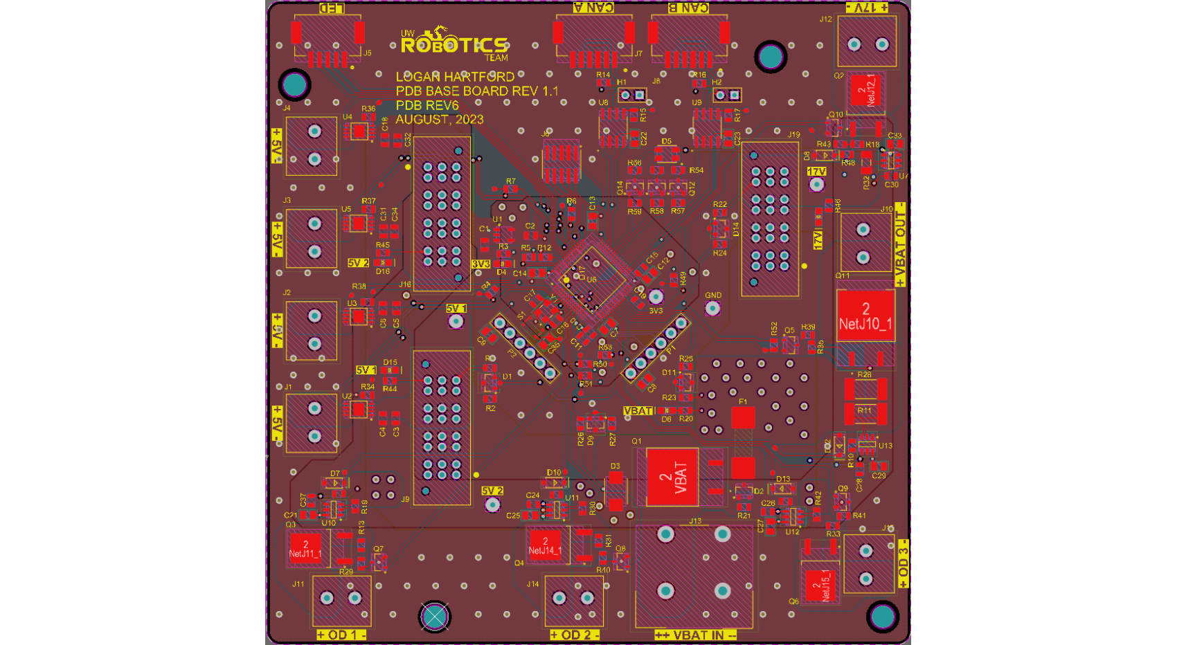
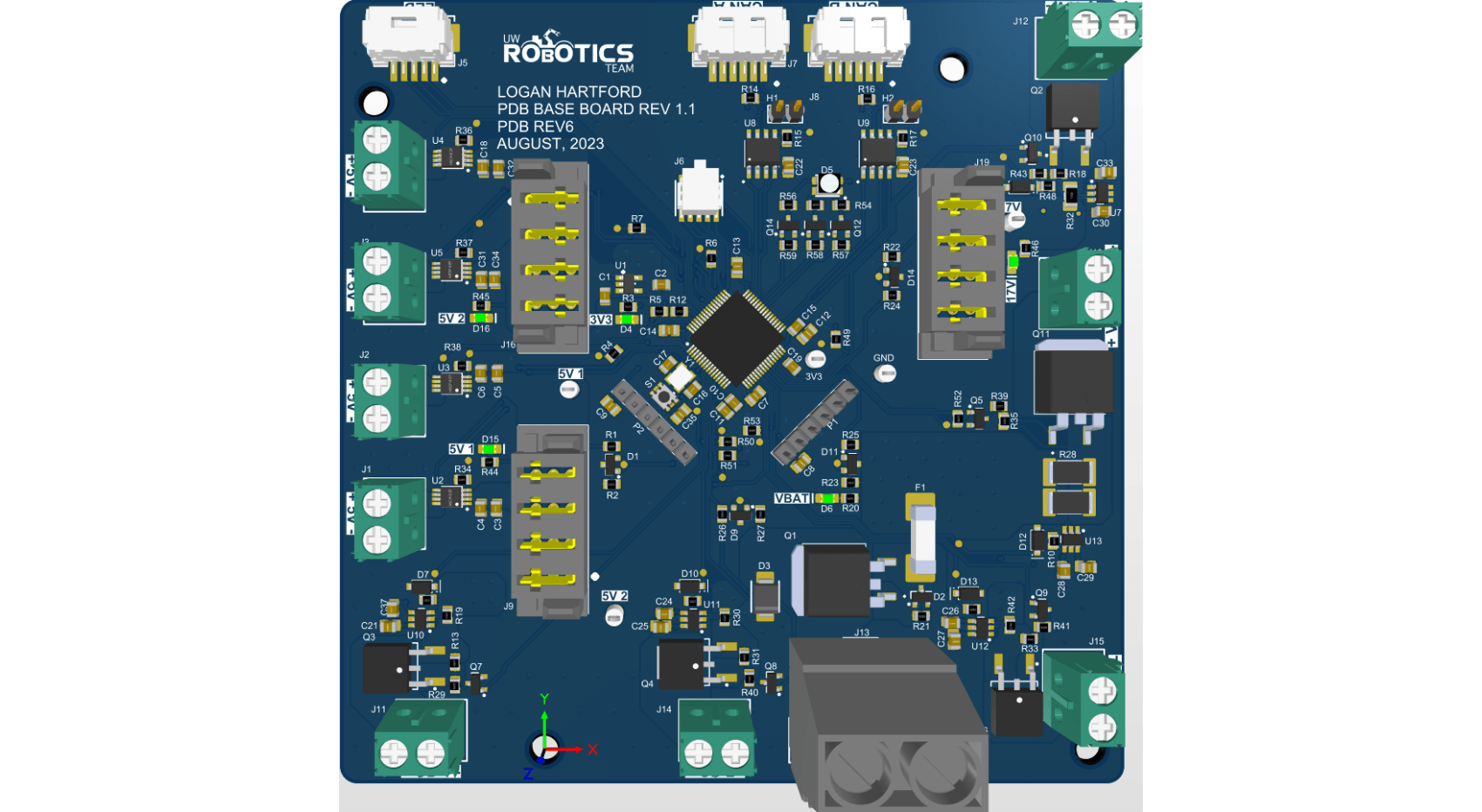
I placed the STM32 and its closely related components on a 45 degree angle because I thought it looked cool.
Routing
I used polygons on all layers. The top layer was my primary routing layer, I used polygons to connect and high power nets, traces for everything else and them pour a GND polygon over all the unused space. I kept layer 2 entirely reserved for GND to provide a close current return pathway.
Layer 3 is primarily ground but I also added in some polygons for connected the 3V3 and 5V nets. The bottom layer is my secondary routing layer, it includes a polygon for the 48V nets and GND polygon everywhere else. I used via stitching to connect polygons of the same net on different layers.
Differential Routing
The CAN traces are routed differentially up until the transceiver. All of the current sense lines are routed differentially.
Buck Module Layouts
The layouts for the 5V and 17V buck converters were created by Melissa and Rayyan respectively. The layouts were created by referencing the data sheet and some layout references they had collected
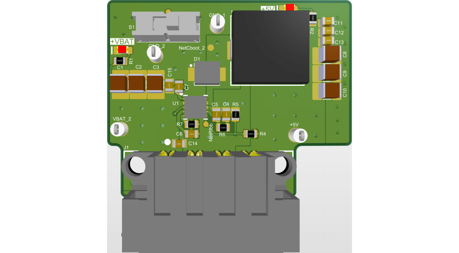
My contribution included teaching them how to use Alitum including how to create a layout, import footprints, routed connections and create polygons. Another major focus was getting the position of the hot loop components correct. I instructed them on general best practices and also checked their work against their design references and the datasheets.
I showed them how to identify the “hot” components in their schematics and how to minimize the distance between these components in layout to reduce the EMI of their designs.
Baseboard Testing
For testing the baseboard, I created and followed test plans for the first and second revisions of the board.
During the testing for the first revision, I focused mainly on testing the electrical functionality of the circuits I added to the design. The testing was pretty straight forward. It mostly involved applying loads to the various output channels and ensuring the correct signals were being generated in over current conditions. I also verified that the STM32 could be program and wrote some simple scrips to test that the STM32 was reading the important signals correctly.
Many small errors were discovered during testing (noted in the test plans above). The show stoppers which forced a second revisions were:
- A bad N-CH footprint in the team library.
- A bad pushbutton footprint in the team library.
- Improperly sized protection diodes on the current sense amplifier outputs.
I added TVS diodes to the current sense outputs because the output of the amp could exceed the maximum allowable voltage of the STM32 pin. My mistake was not adding a current limiting resistor. This meant that when the reverse breakdown voltage of the diode was reached, the diode essentially became a dead short to GND and the current would damage the diode and cause it to fail open circuit, leaving the STM pin unprotected.
I also realized that the breakdown of the original diode was 5V not 3V so in the next revision I changed it to a 3V diode and added a current limiting resistor. The testing of the second revision went smoothly, no show stoppers.
Buck Module Testing
For testing the baseboard, Melissa and Rayyan created and followed test plans for the 5V and 17V bucks. I helped them create their test plans, taught them how to assemble their boards and showed them how to use the testing equipment we have in out lab.

I had them collect a set of performance data and calculate performance parameters like:
- Line regulation
- Load regulation
- Efficiency
- Output ripple
- Transient response
- Operating Temperature
The results from their testing were used to inform the changes for the next revision.
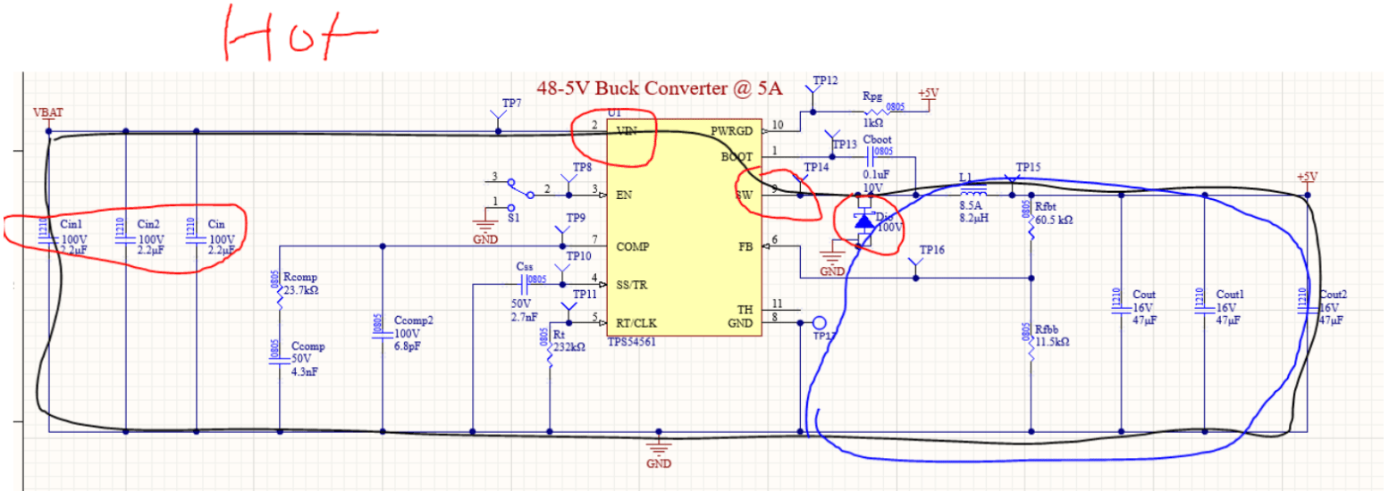
5V
The 5V buck suffered from some excessive ripple at the output as well as poor efficiency. Using the thermal camera, we discovered that the flyback diode was getting very hot during operation. We changes out the diode for one with a lower voltage drop for Rev2. The ripple was addressed by adding some additional capacitance at the input and outputs, as well as adding some different sized capacitors to filters out additional frequencies of noise. We also re-tuned the compensation network values.

These changes led to a much better result for the second revision. The second revision had much better efficiency and much lower ripple.
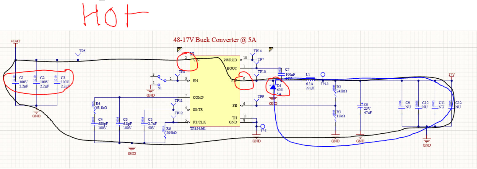
17V
17V buck also suffered from excessive ripple and poor efficiency, however the ripple current was much worse than the 5V buck. The efficiency was relieved by making a similar BOM change as was done on the 5V. Resolving the ripple also involved that same steps that were taken for the 17V.
These changes led to a much better result for the second revision. The second revision had much better efficiency and much lower ripple.
Results
By the end of the summer 2023 semester, we had successfully produced the first working revision of the power distribution board. I was a lot of hard work but I am extremely proud of what Rayyan, Melissa and I accomplished thi term. Rayyan and Melissa have also progressed amazingly as hardware designers and I’m sure will be working in the field very soon. In the following semester, Rayyan became co-lead of the electrical sub-team.
Before I left for my co-op I created firmware specifications to guide the development of the PDB firmware.

I left the guide with Yuchen Lin who developed the firmware during the fall 2023 semester. The board has been incorporated into the rover’s architecture and is now a functional and integral part of the rover.