24V Multiphase Buck
This project was completed for the University of Waterloo Robotics Team’s 2022/23 Mars rover.
I completed revision one of this project while I was a member of the electrical sub-team. During my time as the electrical sub-team lead, I mentored a new member during his design of the second revision of the board.

The Mars rover is powered by a 48V battery however, the motors in the Arm system, used for grabbing and picking up objects, require 24V. These motors are under a high load and require a lot of current.
Therefore the goal of this project was to be able to step down 48V to 24V and deliver 30 amps at the output, without setting anything on fire.
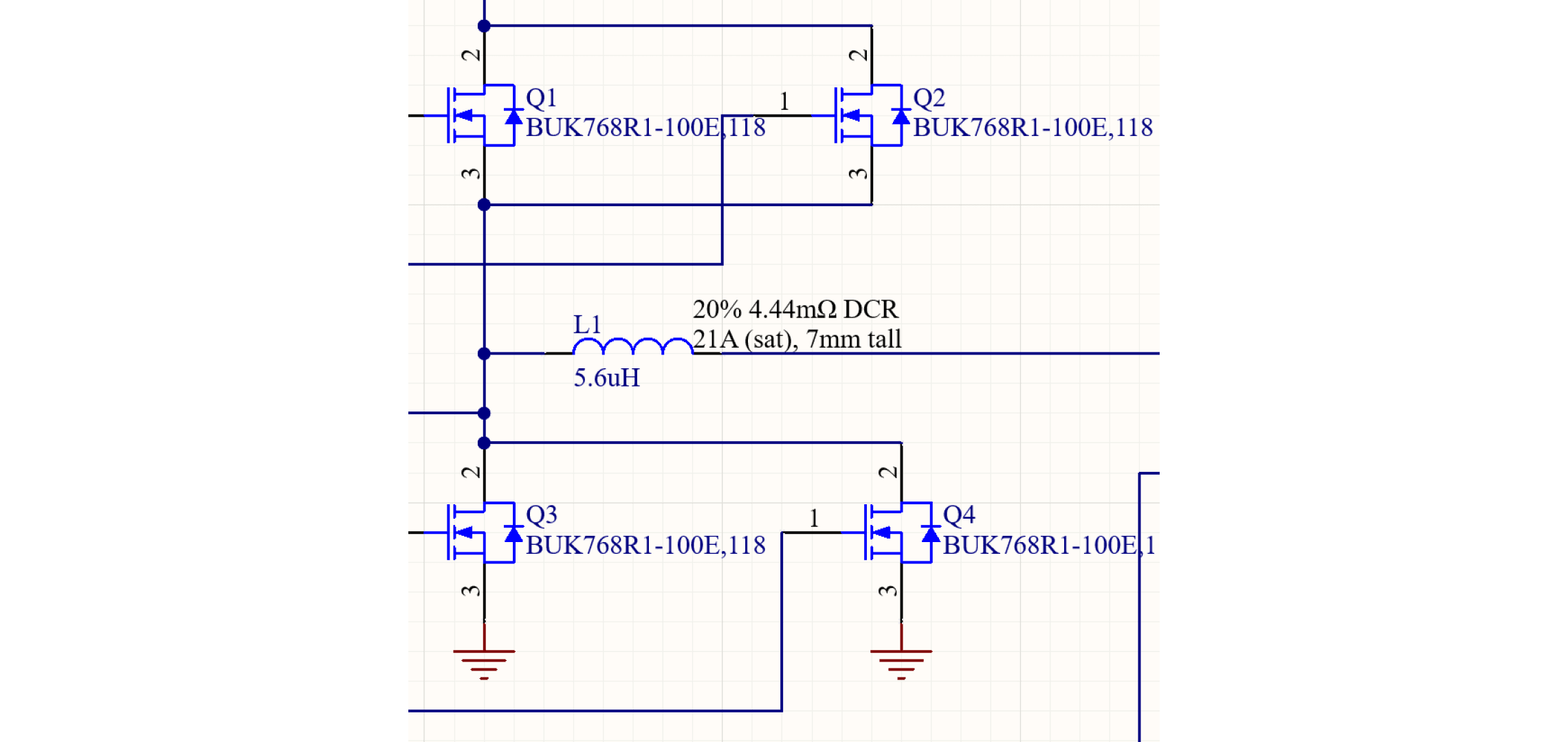
Revision 1 Schematic

Design Constraints and Parameters
- Max input voltage: 50.2V
- Min input voltage: 30V
- Output voltage 24V
- Max load per channel 15A
- Total max load: 30A
- Switching frequency: 361 kHz
The input voltage range is determined by the battery and the max load requirement was given to us by the mechanical team working on the Arm assembly. A switching frequency of 365 kHz was selected as a good balance between ripple and switching losses.
With these parameters defined, the passive component values could be calculated using the formulas provided in the datasheet.
One major oversight in this revision was not calculating the IC power dissipation. These calculations are absent from revision 1 and this neglect will come back to bite.
Design Decisions
For each channel, MOSFETs were placed in parallel because we were worried that in a single FET set-up, the MOSFETs might get too hot.
As mentioned previously, one thing that was overlooked in this design is IC power dissipation which is mainly driven by the total gate capacitance of all of the switching MOSFETs. By having MOSFETs in parallel, we essentially doubled the switching losses on a set of FETs that already had fairly high gate capacitances.
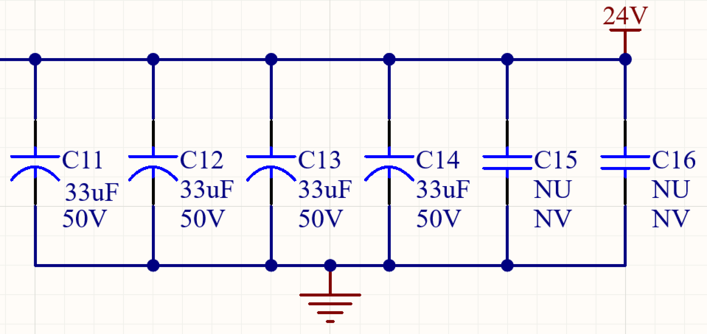
At the output, electrolytic capacitors were chosen due to their availability in convenient sizes for this design. This is the second major oversight of this revision. What I did not consider was how the higher ESR of the electrolytic capacitors would impact the output ripple voltage.
Two blank pads were added to the design in case additional output capacitance was needed.
Revision 1 Layout
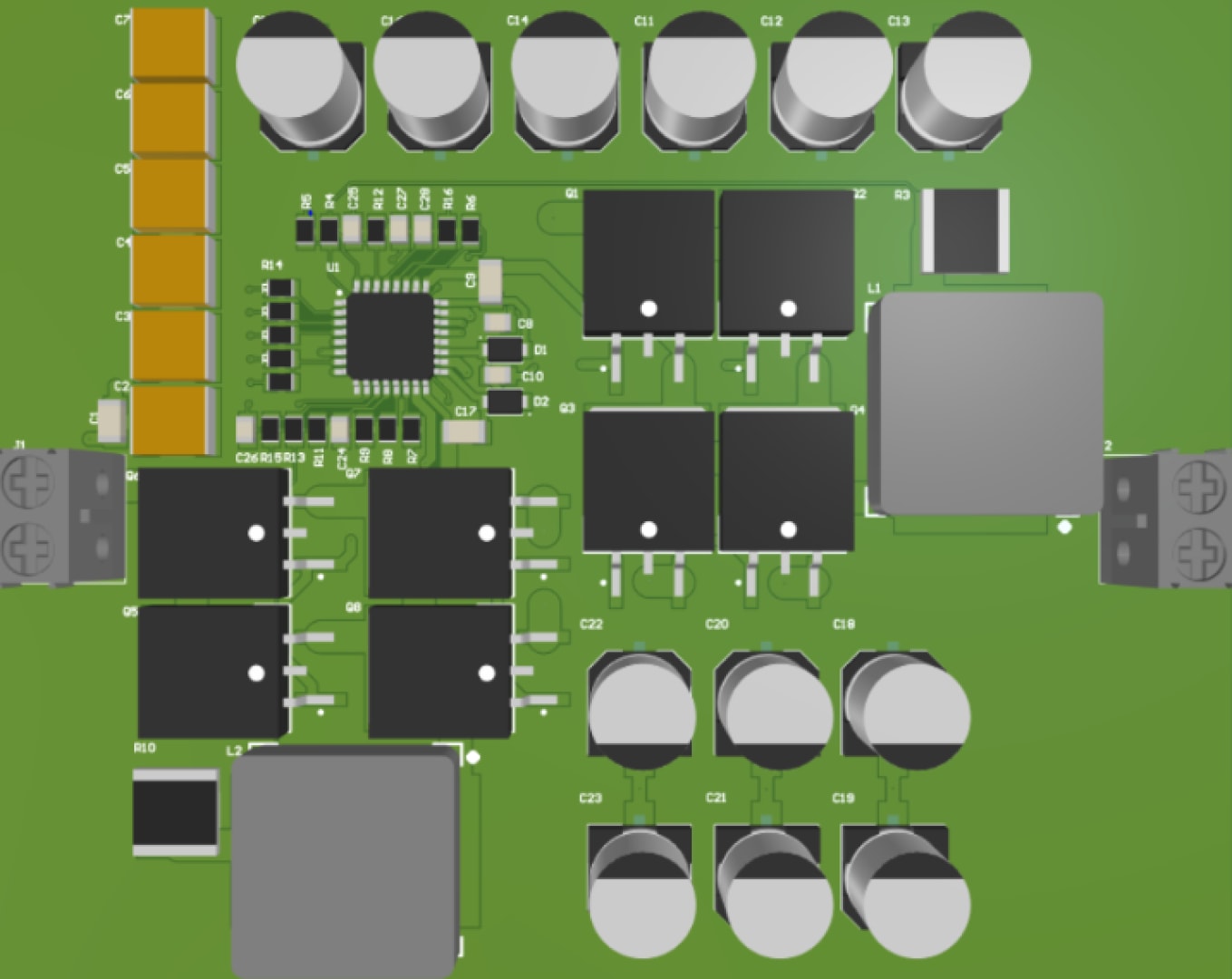
The layout for this design is extremely involved and it took two cycles of design review for me to get something that would work.
My first layout attempt can be seen in 3D below. This is the only evidence I have of this atrocious layout since it was promptly overwritten.
Some of the issues with this layout:
- Not using polygon pours for high-power nets.
- Not routing noise-sensitive current sense and feedback lines away from switching nodes or noisy parts of the board.
- Not placing input capacitors (hot loop) close enough to the MOSFETs to minimize EMI.
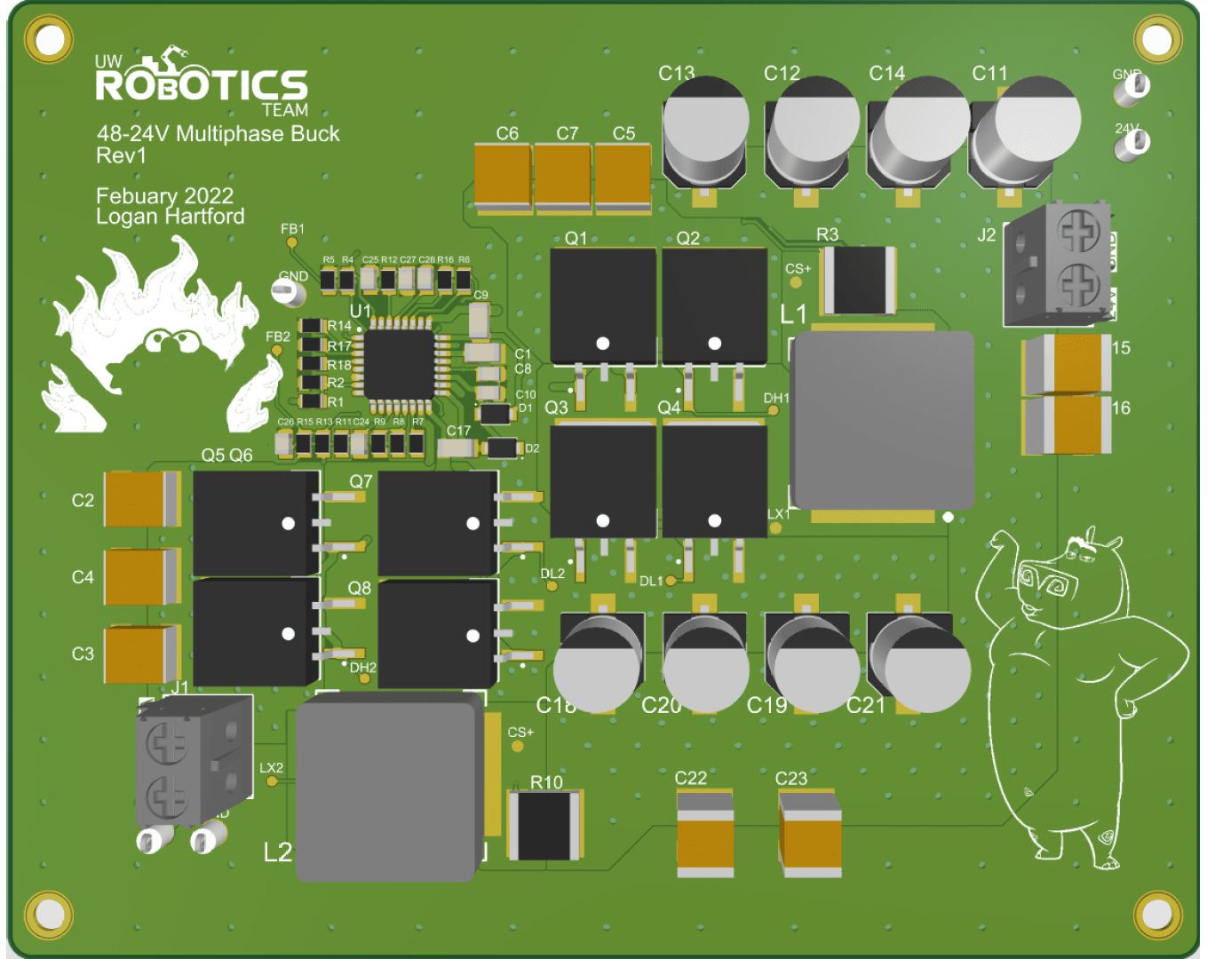
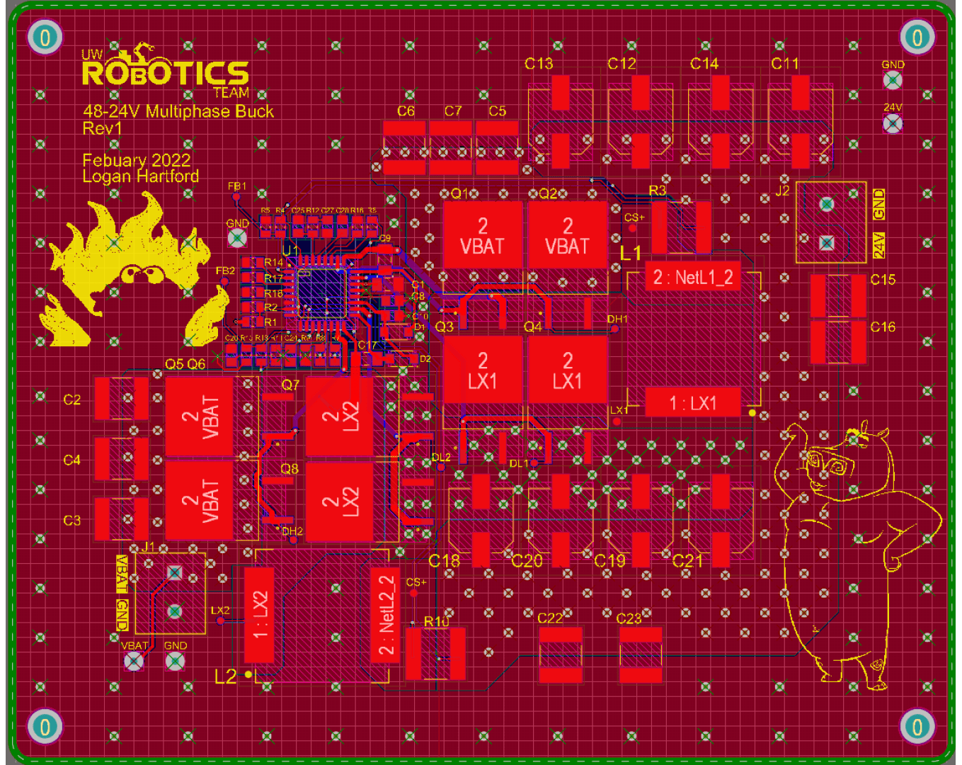
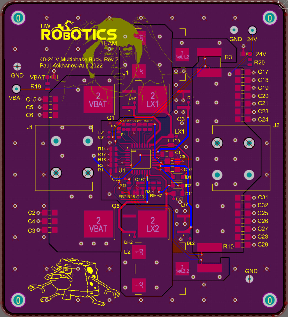
In the second layout attempt, a much better job was done. All of the high-power nets are connected together with polygon pours on the top layer.
The board is 4 layers, with two routing layers and two power planes. One of the power planes is GND and the other is split between VBAT and 24V. All of the polygons that are poured above a power plane with the same net also have via stitching to electrically connect the polygons and the planes together to maximize current pathways.
On the top layer, there is also a GND pour anywhere there isn’t already a polygon or component and the entire bottom side of the board has a GND pour as well to maximize current return pathways.
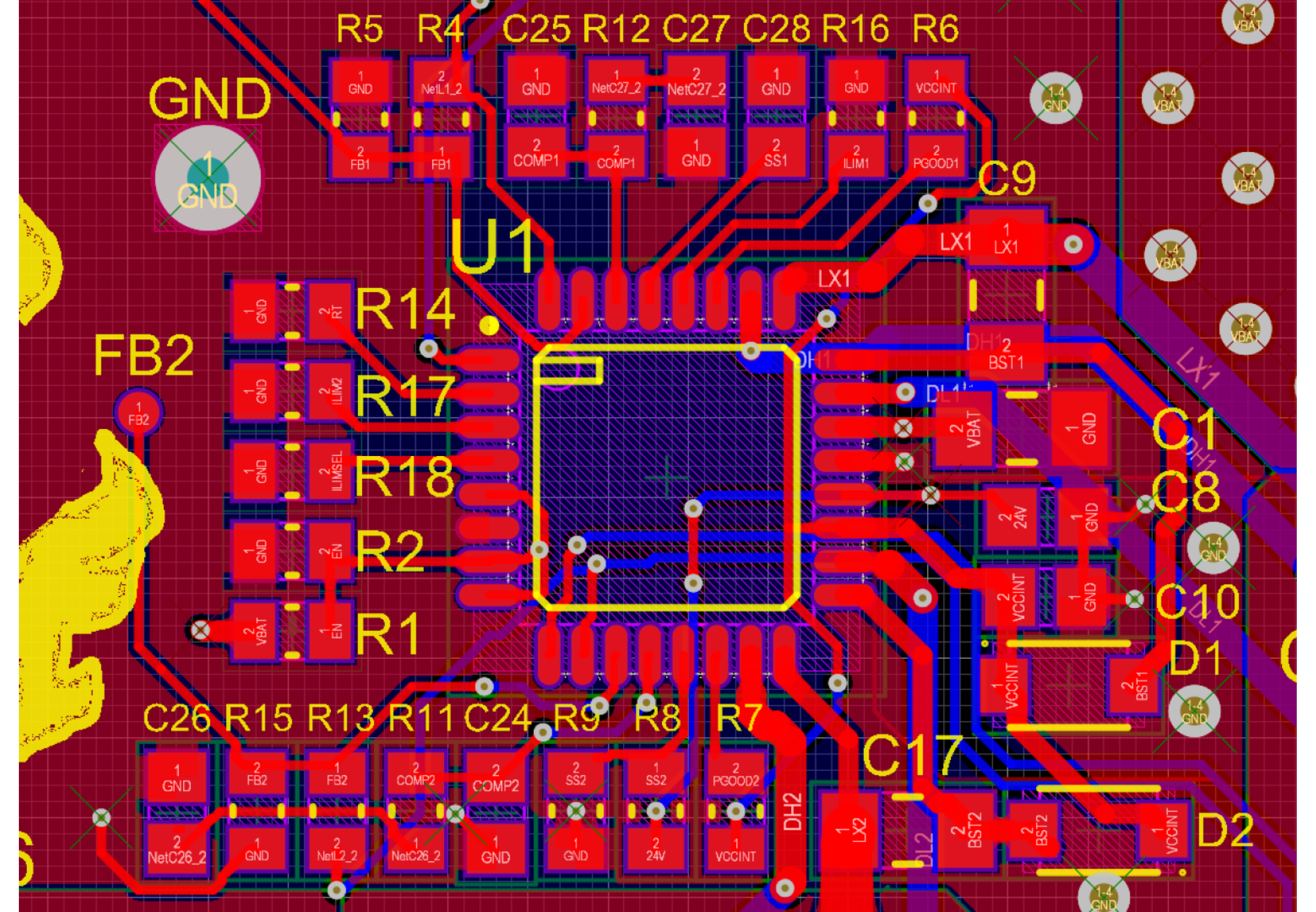
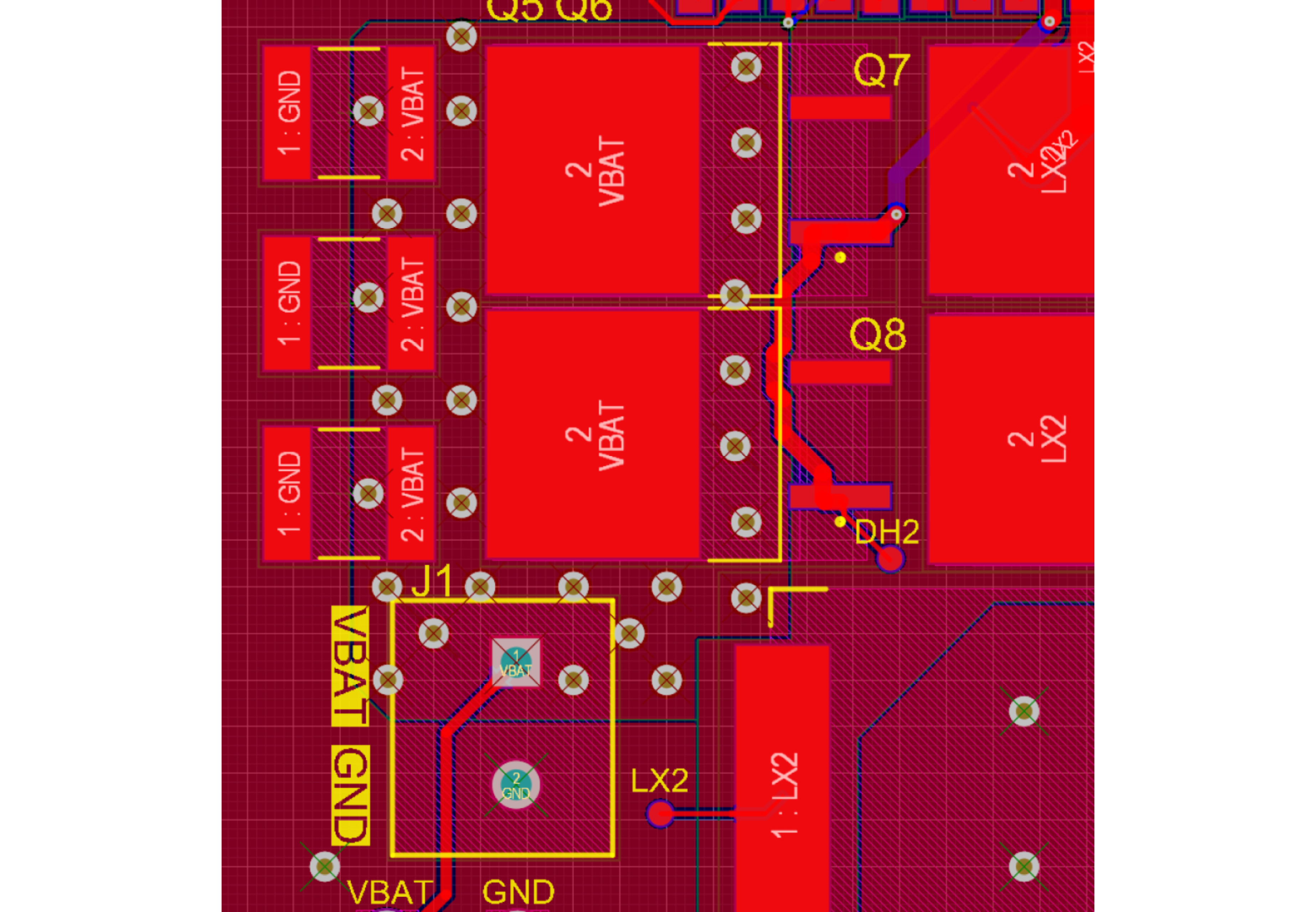
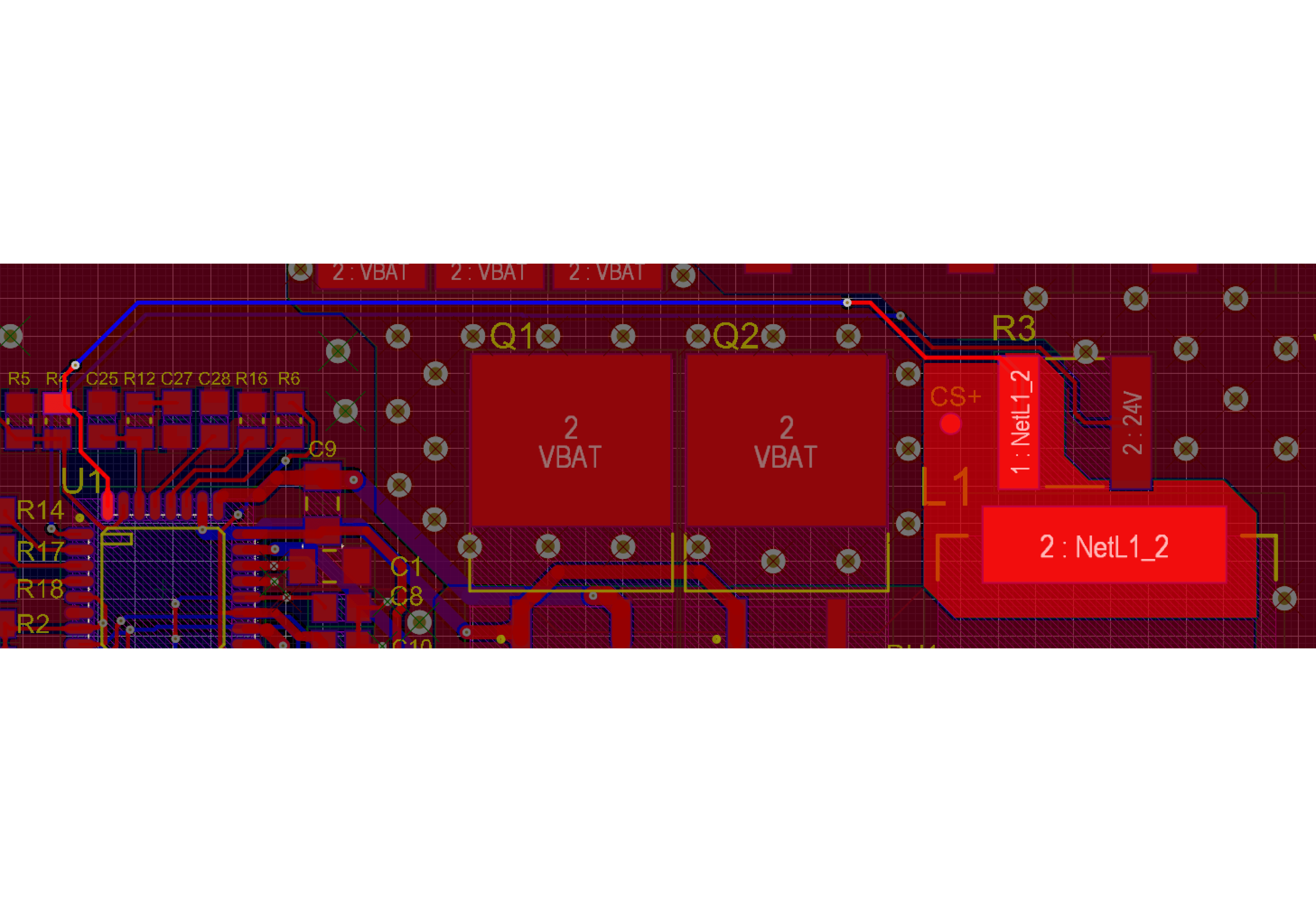
In this version of the design, the hot-loop was properly placed and routed. The only components on this buck that have variable current are the input capacitors so they were placed as close as possible to the switching MOSFETs to minimize trace length and EMI.
The feedback and current sense lines were also routed to the bottom of the board and away from switching nodes to try and prevent any noise from switching from muddying up the signals. The positive and negative lines are also routed differentially.
Mistakes and Changes For Revision 2
Schematic
While working through the datasheet calculations, I forgot to calculate what the IC power dissipation would be in the current set-up. As it turns out, with our dual MOSFET configuration, the IC would be dissipating way too much power.
During testing, we could power up the IC and get 24V at the output but as soon as any load was applied to the output the IC shut down from overheating. The IC was overheating from supplying too much current to the gates of the MOSFETs during switching. The MOSFETs had very high gate capacitances and were in parallel so the IC was having to supply 4W of power to switch the FETs. To get some of the testing done, we changed out the frequency resistor and dropped the switching frequency to 100 kHz so the IC wouldn’t overheat.
Another issue we found was that the ripple at the output was much too high. This was likely due to selecting high ESR electrolytic caps by mistake as well as because we had to lower the switching frequency to perform the tests.
Layout
The major mistake that I made in layout was not placing and routing the two phases of the buck equally. I learned while preparing for revision 2 that the channels of a multiphase buck should have the same length current pathways.
This is to ensure that the switching ripple from each channel interferes destructively and works to reduce ripple current. If the current pathways differ, the ripple may actually be constructively interfering, increasing the ripple at the output.
Not having even channels can also hide power losses occurring in the system since the power being seen at the output is not necessarily representative of both channels.
Changes for Revision 2:
- New MOSFET with lower gate capacitance and higher drain current
- New inductor which is suited to the new configuration
- New ceramic output capacitors
- Make channels of buck symmetric in layout
Revision 2 Schematic

Major Changes
- Sourced a new MOSFET that could be used in a single FET configuration and had a lower gate capacitance.
- Lowered the switching frequency a little bit to meet some of the other design requirements.
- Sourced new ceramic capacitors for the output.
- Added LED indicators to power rails.
- Sourced a new inductor to better suit this configuration.
- Recalculated all of the loop compensation components.
Revision 2 of the 24V Multiphase Buck Converter was completed by Paul Kokanov.
This was Paul’s first ever board design so it was my responsibility to mentor him through the process. Paul started the design by making the necessary changes, updating the calculations and making BOM changes where necessary.
Revision 2 Layout
The biggest changes to this design occurred in the layout.
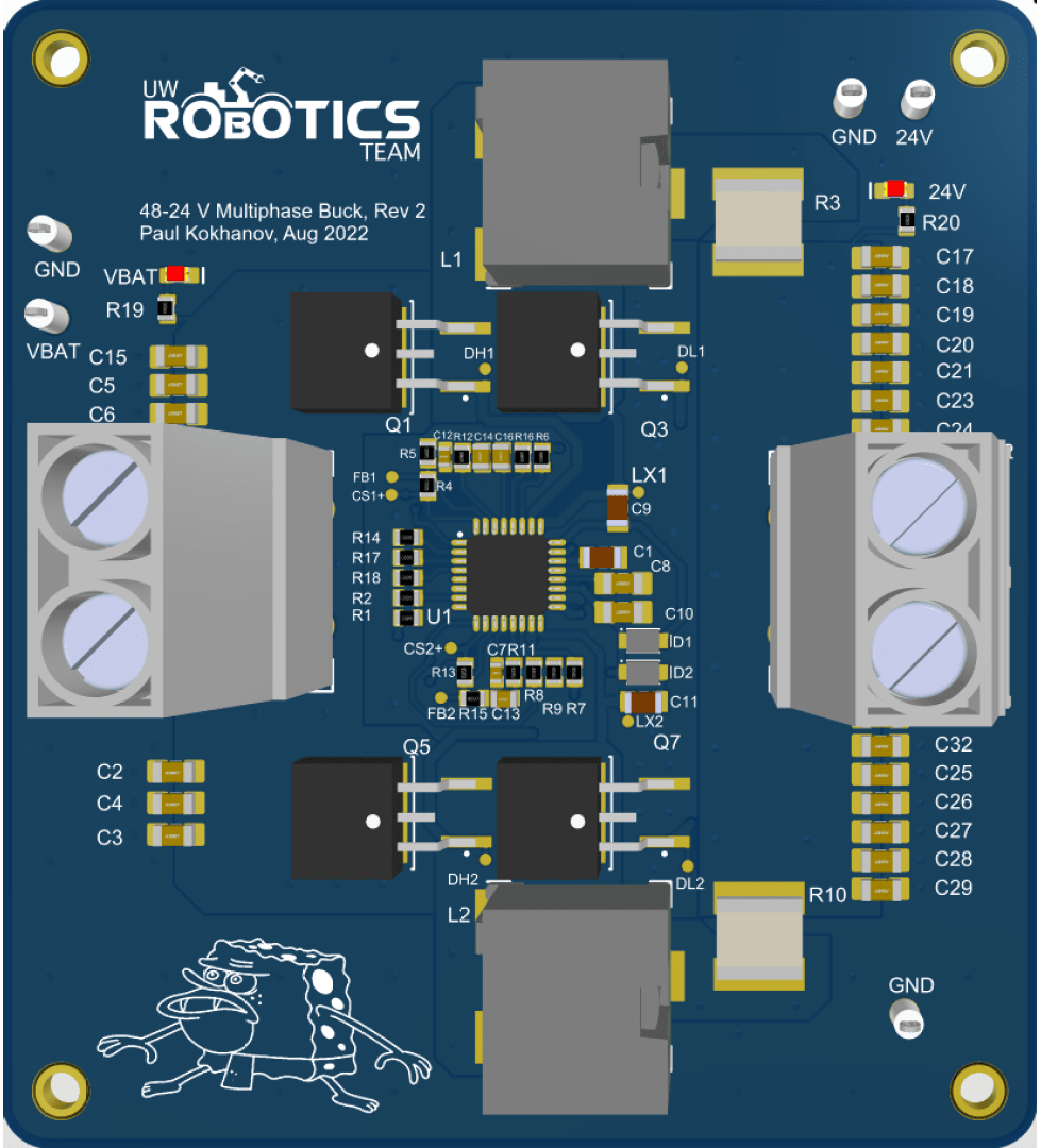
The main goal of this second revision layout was to make the two channels of the buck as symmetrical as possible while still following all the rules of proper buck converter and high power layout.
Revision 2 Results
This revision was a significant improvement on the first. We got rid of the IC over-temp issue and were able to draw a load from the buck without and BOM changes. One major issue is that during layout, Paul and I were referencing the incorrect inductor datasheet while making the footprint so the inductor was far too large for the pad. I had to do some sketchy wiring which certainly negatively impacted the test results.
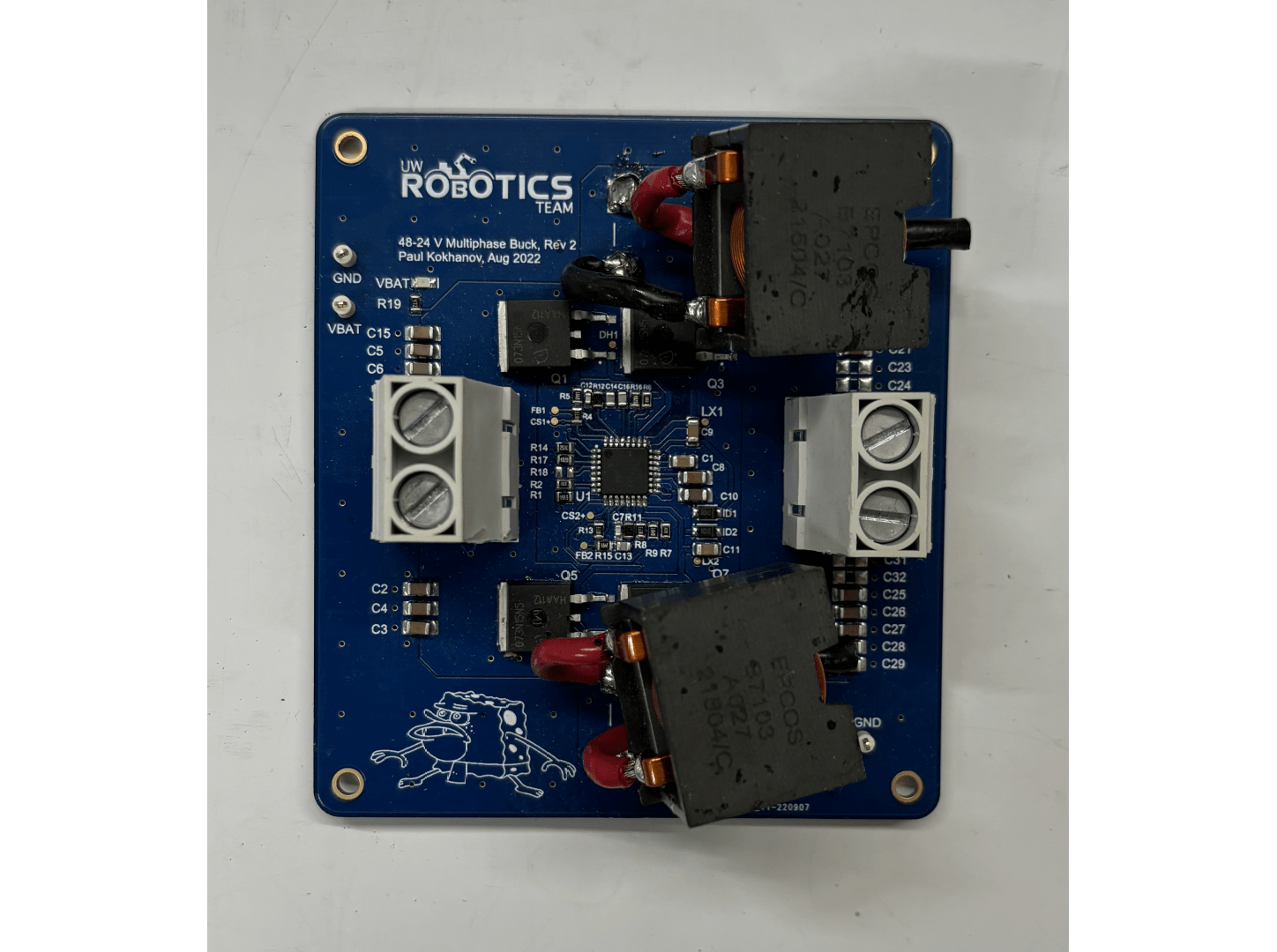

During testing, we were able to draw 8A from the buck before the output would become unstable and shutdown. It appears this was being caused by some runaway interference between ripple current of the two channels which cause the IC to go into a fault mode. This issue was not deeply investigated as priorities needed to be shifted to support drive-train testing.
It was later decided it would be better to modularize the 24V power conversion and avoid the complexities of a multiphase buck converter. The current plan is to supply the 24V motors with 3 separate 24V buck converters, each able to supply 10A. In this design, we created the schematic from the datasheet but in this modular version, we decided to make use of WeBench to alleviate some of the design work. This version is currently being worked on by Muhammad Tanveer and as of January 1st, 2024 revision 1 is complete.
I am not intimately involved in this project as I have moved on to more system level leadership, so this report ends here.